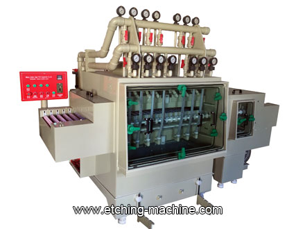
PCB photoresist developing system
Features:The PCB photoresist developing system is designed for PCB photoresist film development, featuring auto spray imaging and a high-precision oscillation system.
Working Principle
The PCB developing machine works by spray developing solution to remove unexposed photoresist from a circuit board. After UV exposure, the machine uses chemical developers to dissolve the unwanted resist, revealing the circuit pattern. Adjustable settings control temperature, spray pressure, speed and time for precise development and accuracy.
Process Flow: Load → Develop → Rinse → Dry → Unload
Main Technical Parameters:
– Model: GE-SRD650
– Power: 3KW/380V
– Conveyor Widths: 400/650/800/1000/1200/1500mm
– Working Height: 720±10mm
– Developing Area Length:1000mm
– Rinse Area Length: 200mm
– Working Temperature: 38~65°C
– Tolerance: 0.05mm
– Developing Type: Double side spray with oscillation system
– Dimensions: 2550x1600x1400mm
– Weight: 300kg
Control Systems:
– Speed Adjustment
– Pressure Adjustment
– Temperature Control (Heater)
– Network Filter System
– High-temperature PP Material (up to 100°C)
– Long-time working Capability
Common Processes:
– Developing (Stand Alone)
– Developing → Rinse → Drying
– DES (Develop → Etch → Strip)
– Custom Sizes (1 to as many chambers as needed)
Common Chemicals:
– 1% Potassium Carbonate
– 1% Sodium Carbonate
Applications:
– PCB Manufacture
– Metal Etching
– Electroplating
– Electroforming Stickers
Compatible Resists:
– Dry film photoresists
– Liquid photoresists
– Solder mask resist (dry and liquid)
Machine video:
Contact Us Now!
Karen online Get quick respond !
Email : etchmachinery@gmail.com
WeChat : +86 15010608128
Whatsapp: +86 15010608128
Related equipment :
Photoresist Developing Machine
more PCB machine pls visit:https://www.etchmachinery.com


Reviews
There are no reviews yet.